
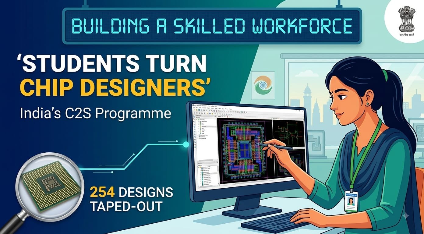
India is taking a major step towards becoming a stronger player in the global semiconductor industry. More than 68,000 students have already received training in semiconductor chip design under the government’s Chips to Start-ups, or C2S, programme. Along with this training, students and academic institutions have successfully taken 254 chip designs to the tape-out stage.
The development is important because semiconductors are used in almost every modern device. Mobile phones, computers, electric vehicles, medical equipment, defence systems, renewable energy devices and artificial intelligence technologies all depend on chips. As demand for these products increases, countries need skilled engineers who can design and develop advanced chips. India’s programme is aimed at preparing such talent within the country.
The Chips to Start-ups programme was introduced to reduce the shortage of trained professionals and improve access to chip-design infrastructure. It is designed to create around 85,000 industry-ready professionals at the B.Tech, M.Tech and PhD levels. The focus remains on giving students practical experience rather than limiting learning to classroom theory.
A chip passes through several stages before it can be used in a real product. One important stage is known as tape-out. In simple terms, tape-out means that the final design has been prepared and sent for manufacturing. It does not mean that a finished commercial chip has already reached the market, but it shows that the design has moved beyond the basic planning stage and is ready for fabrication.
Under the programme, 175 student-made designs were taped out at the Semiconductor Laboratory in Mohali, Punjab. These designs were made using the 180-nanometre technology node. Another 79 designs were taped out at overseas semiconductor foundries. Together, these numbers bring the total to 254 student chip designs.
The programme is also helping students gain access to professional electronic design automation tools. These tools are used by engineers to create, test and verify chip designs before manufacturing. Companies such as Synopsys, Cadence, Siemens EDA, Ansys, Keysight, Silvaco and AMD Xilinx have contributed tools, training support or technical assistance. This gives students an opportunity to learn with systems that are used in the professional semiconductor sector.
The training network covers hundreds of academic institutions. The Prime Minister’s Office has stated that 315 universities are training students in complex chip design with the help of advanced design tools. This approach allows students in different parts of the country to participate in India’s semiconductor mission, instead of concentrating opportunities only in a few major technology centres.
The programme is expected to support both employment and innovation. Students trained in chip design may find opportunities in electronics, telecommunications, automotive technology, defence, space research, energy systems and artificial intelligence. Some may also use their skills to develop products through start-ups, which explains the connection between chips and start-ups in the programme’s name.
India’s semiconductor plans are expanding beyond design. The next stage is expected to place greater emphasis on clean-room operations, semiconductor fabrication, chip packaging, testing and other manufacturing-related skills. This is necessary because designing a chip is only one part of the larger semiconductor supply chain.
The progress also reflects a wider change in India’s technology education. Earlier, many students studied electronics and computer science without access to expensive chip-design facilities. Government-supported access to tools, laboratories and expert guidance is helping bridge that gap. A student sitting in a college classroom can now work on a design that may eventually be tested and manufactured through an organised national programme.
However, training numbers alone will not guarantee success. Continued investment, stronger links between universities and industry, advanced laboratories and opportunities for internships will be needed. The quality of training will be just as important as the number of students enrolled.
Still, the achievement of training more than 68,000 students and taking 254 designs to tape-out shows that India is building the foundations of a domestic semiconductor ecosystem. The effort could help create skilled jobs, encourage technology start-ups and reduce dependence on foreign sources for critical chip-design capabilities.

